
Article contents0%
- Source note
- The short answer: architecture beat silicon
- Two generations, two trade-offs
- Decision 1 — merge the workshops
- Decision 2 — never compute what you already computed
- Decision 3 — tune one screw at a time
- Where the 129 ms goes: the bandwidth wall
- The PPA scorecard
- Success was verified harder than failure
- What it still gets wrong (and why that matters)
- Why embedded-AI buyers should care
- Sourcing the XC7Z020 and Zynq-7000 family
- The bigger "so what": small Transformers are a real track
- Conclusion
- Sources
Source note #
This article is a LimChip English rewrite and procurement analysis based on the 网络交换FPGA WeChat series 《把大模型塞进FPGA》 and the linked open-source project repositories.
The short answer: architecture beat silicon #
For years the story of on-device AI has been "get a bigger chip." A university course in China just showed the opposite. Eight students took the same exam a previous cohort had failed on a large AMD Xilinx Zynq UltraScale+ xczu7ev board — port a 6-layer nanoGPT (Shakespeare corpus, 384-dim, 65-token vocabulary) onto an FPGA — but sat the new cohort on a much smaller Zynq-7000 XC7Z020 dev board.
In this reported project configuration, the XC7Z020 build reached approximately 6.0× lower token latency than the earlier XCZU7EV implementation (129.5 ms vs 777 ms per token), while using approximately 4.3× lower LUT usage in the reported implementation. That is not a typo: a chip about eight times smaller by resource turned in six times the latency improvement. The combined LUT and latency comparison produces an approximately 48× product difference in this reported implementation; it is not a general device rating. For anyone sourcing FPGAs or building edge-AI prototypes, the lesson is worth the read.
Two generations, two trade-offs #
The previous cohort spread the Transformer across 11 dedicated accelerator IPs — one per operation (LayerNorm, attention, matmul, FFN, and so on). On a large device with spare silicon, that "area-for-speed" layout is easy. The new cohort, on a device with a fraction of the logic, tore those blocks down and kept one shared compute core, scheduled by a state machine so Q/K/V projection, attention, residual and FFN all take turns on the same multiplier block. The industry term is time-division multiplexing.
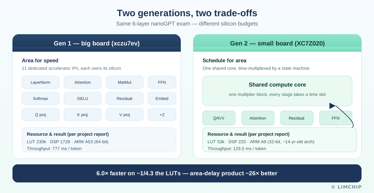
Resource and result figures below are per the project's post-route Vivado report:
| Gen 1 (xczu7ev) | Gen 2 (XC7Z020) | |
|---|---|---|
| LUT | ~230k | ~53k (51.9% used) |
| DSP | 1728 | 220 (114 used) |
| ARM core | 64-bit A53 | 32-bit A9 (~14-yr-old architecture) |
| Token latency | 777 ms | 129.5 ms |
BRAM was the tightest resource on the small board at 77.9% — close, but it closed. The point for buyers: a constrained part forced the discipline that a large part let the team skip.
Decision 1 — merge the workshops #
Collapsing 11 accelerators into one shared core is the single biggest reason the small board worked at all. It costs scheduler complexity (writing the state machine takes a clear head), but it let a 6-layer Transformer fit with LUTs barely past half. This is the everyday craft of ASIC and FPGA engineers: making one square metre do the work of three. When you scope an edge-AI design, ask whether your BOM is buying *silicon* or *schedule discipline* — the second is cheaper and the first is often a convenience.
Decision 2 — never compute what you already computed #
The highest-value move was the simplest. A generative model recomputes attention against every prior token; a token's Key (K) and Value (V) never change once calculated. The previous cohort recomputed all prior K/V for every new token — correct, but wasteful. The new cohort stored K/V in DDR memory (a K/V cache) and only computed the new row. The whole 6-layer notebook occupied about 1.1 MiB of memory and removed ~100× redundant math.
That is the same idea behind vLLM and TensorRT-LLM — reproduced by undergraduates on a teaching board. One detail they handled that production stacks also handle: when the quantization scale changed, the cache was flushed wholesale rather than reusing mismatched old data. The ARM program managing all of this was under 30 KB of code and data.
Decision 3 — tune one screw at a time #
Rather than a big rewrite, the team iterated in four signed-off steps (board-measured means, not simulation):
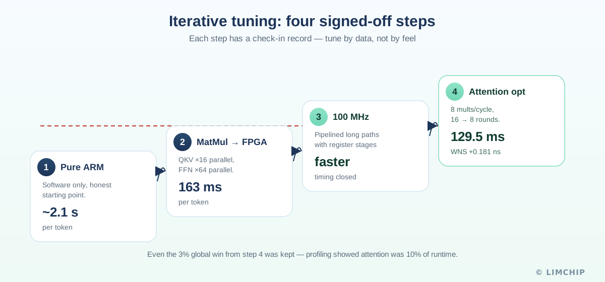
1. Pure ARM software — about 2.1 s/token. An honest baseline. 2. MatMul into FPGA — Q/K/V projection 16-way parallel, FFN 64-way parallel — down to 163 ms. 3. Frequency to 100 MHz — long combinational paths were cut with register pipelining so timing closed. 4. Attention optimization — 8 multiplies per cycle, 64-dim head from 16 rounds to 8 — final 129.5 ms/token, timing report WNS +0.181 ns, TNS 0.
Step 4 bought only ~3% globally, yet they shipped it because profiling showed attention was ~10% of runtime. Tune by data, not by feel — a habit worth more than any specific tool.
Where the 129 ms goes: the bandwidth wall #
Optimizing for three weeks only moved matrix-multiply's share from 95.5% to 90.8% of runtime. The reason is structural: generating each token means moving tens of millions of weights from memory. Faster compute does not help if the mover is the bottleneck. The team named it directly — the bandwidth wall, the same wall every AI accelerator hits. Their next target is already flagged: FFN alone is ~48.7% of runtime.
For buyers this is the durable takeaway: on edge AI, memory bandwidth and capacity often matter more than peak MAC count. A part with more multipliers but slower, smaller memory will lose to a tighter part with better data movement.
The PPA scorecard #
Chip work is judged on three letters — Performance, Power, Area. The project cashed every decision into numbers:
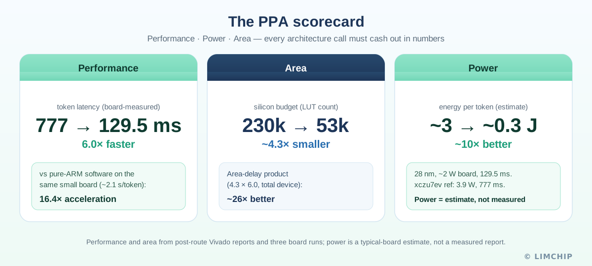
- Performance: 777 ms → 129.5 ms (≈6.0× lower latency, based on the reported implementation and test conditions); versus pure-ARM on the same small board (~2.1 s) that is 16.4×. All board-measured.
- Area: ~4.3× lower LUT usage in the reported implementation; area-delay product ~26× better (based on the reported implementation and test conditions, 4.3 × 6.0 across total device resources).
- Power: prior xczu7ev reported ~3.9 W (≈3 J/token); the small 28 nm board draws ~2 W, so ≈0.3 J/token — an estimated improvement of roughly 10× under the project's stated board-power assumptions, driven mostly by the 6× speed-up.
One honesty note from the report we keep: power is a typical-board estimate, not a measured report for this project. Performance and area come from post-route Vivado reports and three board runs.
Success was verified harder than failure #
The previous cohort's most cited moment was an honest "FAIL" printout. This cohort had no FAIL — and doubled down on verification: simulator operator-by-operator alignment (zero mismatch across all six layers), byte-by-byte comparison of 4,224 intermediate bytes against the golden reference (0/4224), end-to-end 200-token generation against the fixed-point reference (0/200), and three identical reruns to rule out a lucky run. The INT8 perplexity regression was reported at 4.06% using the *same strict bit-exact path as the board* — they noted a looser method would look better and declined to use it. The bitstream and program ship with SHA-256 checksums.
For procurement, the transferable lesson is boring but bankable: demand a verification chain, not a demo video. Ask for the golden-reference comparison, the timing report, and the checksum — especially on custom FPGA or ASIC deliveries.
What it still gets wrong (and why that matters) #
Feed it "everything with a man" and the 200 characters are Shakespeare-flavoured nonsense — invented words, repeated "sea/world/war" loops. Every token is bit-exact against the math, yet the model's grasp of language is the limit of a 10-million-parameter model trained only on Shakespeare with 65 characters. Correctness of implementation and capability of the model are two different exams. Hardware engineers ace the first; the second needs a bigger model, more data, and — as the report argues — a verification layer so the system knows when it should not be trusted.
Why embedded-AI buyers should care #
Three reader lenses from the report, with our sourcing gloss:
- Curious readers: a few-hundred-dollar teaching board proves large models are not mysterious cloud-only magic. FPGA is a rewritable "blank chip" — undergraduates loaded a Shakespeare-writing model and can show you every bit.
- Students / career-changers: the value is a rare full-stack pass — Python training → INT8 quantization → HDL → timing closure → bare-metal driver → board verification. "Ran a Transformer on FPGA and passed token-by-token alignment" beats ten course certificates.
- Practitioners: a few-dollar board reproduces the core contradictions of production LLM-inference silicon — bandwidth wall, area-vs-schedule trade-off, KV-cache cost, quantization honesty.
Sourcing the XC7Z020 and Zynq-7000 family #
The board in the project is the AMD Xilinx Zynq-7000 XC7Z020 — a 28 nm SoC pairing a 32-bit ARM Cortex-A9 with 7-series FPGA fabric. It is a long-lived, widely second-sourced family, which is good for buyers but also a counterfeit-risk family because of its age and volume.
| Check item | What to confirm |
|---|---|
| Exact part number | XC7Z020 has many suffixes (e.g. -1/-2 speed, -CLG400/-SBG485 package, C/I/E temperature). Confirm the exact orderable code. |
| Package & MSL | Verify ball pitch, package code and moisture-sensitivity level before reflow. |
| Date code | Zynq-7000 is mature; confirm an acceptable year/week range and that the part is not a pulled/scrap reclaim. |
| Traceability | Require lot consistency and supplier documentation; the family's age makes fake and refurbished parts common. |
| Lead time | Mature Xilinx parts can still stretch when allocation hits; confirm current quoted lead time before BOM commit. |
Procurement caveat: the XC7Z020 used in this project is a specific device and board configuration. Its measured speed, power and resource usage reflect this reported implementation and test conditions, and do not represent all Zynq-7000 family members. Before you buy, confirm the exact orderable part number — speed grade, package and temperature grade — plus the specific board revision and the Vivado project constraints; ranges and suffixes vary widely across the family.
LimChip's catalogue does not yet list XC7Z020 or other Zynq-7000 entries, so we are not pointing you to a stock page here. If you need XC7Z020, Zynq-7000 siblings, or a Zynq UltraScale+ part for an edge-AI build, open an RFQ and we will source against an approved manufacturer and suffix.
The bigger "so what": small Transformers are a real track #
The report answers the fair challenge — "what is the point of such a small model on FPGA?" — with a literature scan. Three layers are moving at once:
- Tiny task Transformers are near deployment. 4-bit models on smaller-than-XC7Z020 Spartan-7 parts already do forecasting, classification and anomaly detection at sub-millijoule cost; vision Tiny Transformers on ZU boards beat an ARM A53 by ~10× in speed and ~7× in efficiency.
- 0.5B–1.7B edge models are in prototyping. TinyLlama 1.1B on ZCU102, Qwen2.5-0.5B on KV260, and sub-2-bit experiments all show edge SLMs are now about "how to run them worthily," not "whether."
- 7B–8B are probing the embedded limit. LLaMA2-7B on a 4 GB KV260 and LLaMA3-8B via weight-offload reach a few token/s with memory bandwidth near its ceiling.
A reader's satellite question — can an FPGA run an orbital VLM like NASA JPL's Gemma-3-4B demo? — gets a calibrated answer: a high-end FPGA (or FPGA+GPU/NPU) can, by splitting vision encoder + mmproj + 4B decoder, but the 2.4 GB Q4 model plus runtime and KV cache excludes the 512 MB teaching board. Spiking/event-driven vision front-ends can cut the frontend further. The honest line: the XC7Z020 class cannot host Gemma-3-4B; start with the vision front-end and projection, then attack the 4B decoder.
Conclusion #
The XC7Z020 project is a clean demonstration that architecture beats silicon: a shared time-multiplexed core, a K/V cache, and data-driven stepwise tuning beat simply buying a bigger board — and every claim is backed by a verification chain buyers can actually audit. For edge-AI sourcing, the durable rules are mundane but profitable: weigh memory bandwidth before MAC count, demand a golden-reference verification chain, and confirm exact part-number suffixes on mature, counterfeit-prone families like Zynq-7000. The latency, power and resource figures above are specific to this reported XC7Z020 build and its test conditions, not generic Zynq-7000 performance, so do not apply them to other family members without re-verification.
Building on Zynq, Artix, Spartan or Zynq UltraScale+ and need a verified source? Open an FPGA / Zynq RFQ with your exact part number, quantity and date-code window.
Sources #
- 网络交换FPGA 微信公众号,原文系列《把大模型塞进FPGA》。
- nanoGPT on Zynq — XC7Z020 final project repository.
- My Transformer on FPGA — xczu7ev project repository.
- AMD Xilinx Zynq-7000 product documentation.
- Relevant FPGA transformer research papers (e.g. FlightLLM, DFX, CD-LLM, and related academic work).
All performance, area and power figures are from the reported project implementation and test conditions, not general specifications of the Zynq-7000 family. Power is a board-level estimate, not a full measured power report for this project.
Need stock, date-code or package confirmation?
Send the part number, quantity, target date code and packaging requirements. LimChip will check available lots and RFQ details before you place the order.
Send RFQ