
Article contents0%
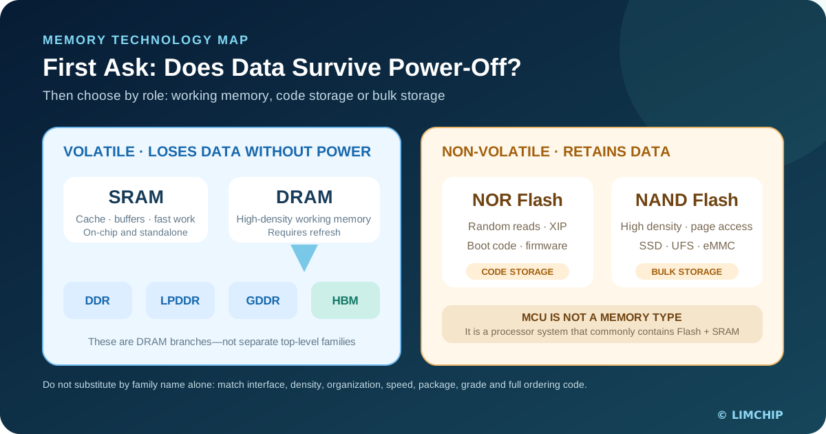
- Start with one question: does the data survive power-off?
- DRAM: the processor's working area
- DDR: a DRAM interface generation, not a separate memory family
- LPDDR and GDDR: two other DRAM branches
- HBM: stacked DRAM connected through an extremely wide interface
- NAND Flash: high-density non-volatile storage
- NOR Flash: random-read and code-storage memory
- SRAM: the fastest working memory, both on-chip and standalone
- MCU: a processor that contains memory, not a memory type
- The one-page translation table
- Procurement: translate the word into an exact ordering code
- Sources and technical basis
Start with one question: does the data survive power-off? #
Most memory terminology becomes easier once the technologies are separated into two families.
- Volatile memory loses its working data when power is removed. DRAM and
SRAM are the main examples.
- Non-volatile memory retains data without continuous power. NAND Flash and
NOR Flash are the two major flash families.
A useful analogy is a desk and a filing cabinet. Volatile memory is the desk on which a processor is actively working. Non-volatile memory is the cabinet that keeps files after the office closes. The analogy explains the role, but it does not mean that every desk or cabinet has the same speed, interface or endurance.
| Family | Retains data without power? | Typical role | Common forms |
|---|---|---|---|
| SRAM | No | Very fast working memory and cache | On-chip cache, standalone SRAM, nvSRAM variants |
| DRAM | No | High-density working memory | DDR DIMMs, LPDDR, GDDR, HBM, discrete DRAM |
| NOR Flash | Yes | Boot code, firmware, calibration and XIP | SPI/QSPI/xSPI NOR, parallel NOR |
| NAND Flash | Yes | High-capacity data storage | Raw NAND, eMMC, UFS, SSD, SD card, USB drive |
These are not interchangeable layers in one universal speed ladder. A NOR device may sit next to DRAM in the same embedded system because one stores boot code and the other supplies working memory. The correct comparison depends on what the system must do.
DRAM: the processor's working area #
DRAM stands for dynamic random-access memory. Each bit is stored as charge and must be refreshed repeatedly. That refresh requirement is why DRAM is volatile: remove power and the stored state disappears.
When a computer opens a document or an application, active code and data are loaded from storage into DRAM so the CPU can work on them efficiently. Phones, servers, network equipment, vehicles and industrial controllers use DRAM for the same broad reason: processors need a large, fast working area.
Calling DRAM “scratch paper” is useful, but raw speed comparisons with an SSD can be misleading. A DRAM channel, an SSD interface and a complete application measure different things. Latency, sequential throughput, random access, controller overhead and queue depth all matter. The safe takeaway is simply: DRAM offers much lower access latency and is optimized for active working data; NAND-based storage offers much higher non-volatile capacity per unit cost.
What “8 GB RAM” usually means #
In a phone or PC specification, 8 GB or 16 GB of “memory” normally refers to DRAM working capacity. A separate “256 GB storage” figure normally refers to NAND-based storage. Marketing sometimes uses the word memory for both, so the technology and function must be checked.
DRAM is supplied by more than three companies. Samsung, SK hynix and Micron are the three largest global suppliers, but Nanya, CXMT and other manufacturers also participate in parts of the DRAM market. Market shares change by quarter and by segment; they should not be turned into a permanent technology definition.
DDR: a DRAM interface generation, not a separate memory family #
DDR means double data rate. Data transfers occur on both edges of the clock, which is the origin of the name. DDR SDRAM is still DRAM; DDR identifies the interface generation and protocol used by common PC and server memory.
DDR2, DDR3, DDR4 and DDR5 are successive standards, but the number is not just a speed label. Each generation changes signalling, voltage, timing, training, power management and physical requirements. A DDR5 device is not a drop-in replacement for a DDR4 device, even if both are described as DRAM.
| DRAM branch | Typical environment | Design priority | Important sourcing fields |
|---|---|---|---|
| DDR3/DDR4/DDR5 | PCs, servers, industrial and network systems | Capacity, bandwidth, platform compatibility | Generation, density, x4/x8/x16 organization, speed bin, package/module type, rank and grade |
| LPDDR4/4X/5/5X | Phones, embedded systems, automotive and compact devices | Power efficiency and board area | Exact generation, voltage option, density, package, temperature grade and SoC qualification |
| GDDR6/GDDR7 | Graphics and high-bandwidth accelerator boards | Per-pin bandwidth | Generation, speed, density, package and GPU/controller qualification |
| HBM2E/HBM3/HBM3E/HBM4 | GPUs, AI accelerators, HPC and high-end programmable devices | Aggregate bandwidth and energy per transferred bit | Stack generation, capacity, stack height, known-good-die status and package/platform qualification |
The familiar desktop DIMM is only one implementation. DRAM can be sold as a discrete BGA, soldered LPDDR package, graphics memory device, registered server module or HBM stack.
LPDDR and GDDR: two other DRAM branches #
LPDDR means low-power double data rate memory. It is designed around power and space constraints and is widely used in mobile, embedded and automotive systems. LPDDR is not a low-power DIMM that can be inserted in a desktop slot; it has different interfaces and packaging practices.
GDDR means graphics double data rate memory. It is optimized for high bandwidth in GPUs and other parallel processors. GDDR and DDR generations do not map one-to-one: GDDR6 is not “DDR6 for graphics,” and ordering codes cannot be compared by the number alone.
HBM: stacked DRAM connected through an extremely wide interface #
HBM stands for high-bandwidth memory. It is a DRAM architecture that stacks memory dies vertically and connects them with through-silicon vias (TSVs) and microbumps. One or more stacks are placed close to the processor, commonly through an interposer or other advanced-package structure.
Conventional DIMM memory connects through a comparatively narrower board-level channel. HBM uses a very wide interface close to the compute die. It can therefore deliver extremely high aggregate bandwidth with favorable energy per bit, at the cost of complex packaging, qualification, yield management and a much higher system cost.
HBM was not invented only for generative AI. It has been used in high-performance graphics, supercomputing, networking and HBM-equipped FPGAs or adaptive SoCs. AI accelerators have made it strategically important because model training and inference can be limited by how quickly weights, activations and KV-cache data move between compute units and memory.
| Attribute | DDR5 module/channel | HBM stack/system |
|---|---|---|
| Physical relationship to processor | Board-level memory channel | Stacked DRAM placed beside the compute die in an advanced package |
| Interface strategy | Narrower, higher per-pin rate | Very wide interface across many channels |
| Main advantage | Capacity, modularity and mature ecosystem | Very high aggregate bandwidth and energy efficiency per bit |
| Main limitation | Board routing and channel bandwidth | Advanced packaging cost, yield, thermal design and limited interchangeability |
| Procurement unit | Discrete DRAM or module | Qualified stack/package/platform supply chain |
Avoid fixed claims such as “one DDR5 module is 50 GB/s and one HBM device is 1,200 GB/s” without a configuration. Module width, channel count, data rate, HBM generation, stack count and processor implementation determine the real bandwidth.
HBM market leadership also changes by generation and quarter. SK hynix is a leading supplier, with Samsung and Micron also shipping and qualifying advanced HBM products. A single unsourced “90% market share” figure should not be used as a permanent description.
NAND Flash: high-density non-volatile storage #
NAND Flash retains data without power and is optimized for high density and low cost per bit. It is the underlying storage medium in SSDs, eMMC, UFS devices, memory cards and many USB drives.
Raw NAND is not normally presented to a host like byte-addressable RAM. It is organized into pages and blocks and requires management for error correction, bad blocks, wear levelling and garbage collection. Those functions may be handled by an SSD, eMMC or UFS controller, or by the host in an embedded design.
SLC, MLC, TLC and QLC #
These labels describe the number of bits stored in each NAND cell.
| NAND cell type | Bits per cell | General trade-off | Typical use pattern |
|---|---|---|---|
| SLC | 1 | Highest endurance and margin, lowest density | Specialized industrial and high-endurance uses |
| MLC | 2 | Higher endurance than TLC, lower density | Legacy and selected endurance-focused products |
| TLC | 3 | Strong balance of cost, density and endurance | Mainstream client and enterprise SSDs, embedded storage |
| QLC | 4 | Higher density and lower cost per bit, tighter endurance margin | Read-heavy, capacity-oriented client and data-center storage |
More bits per cell generally increase density and reduce cost, while narrowing voltage margins and increasing controller/ECC demands. That does not mean every QLC SSD is unreliable or every MLC device is superior. NAND generation, controller, over-provisioning, workload, firmware and qualification determine the finished product.
Modern enterprise SSDs commonly use qualified TLC and increasingly use QLC for suitable workloads. “Enterprise still mainly uses MLC” is no longer a safe generalization.
NOR Flash: random-read and code-storage memory #
NOR Flash is also non-volatile, but its array and interface are suited to fast random reads and code access. Serial NOR devices commonly connect through SPI, QSPI or xSPI interfaces; parallel NOR remains relevant in some systems.
The distinctive concept is execute in place (XIP). When the host controller supports memory-mapped access, it can fetch instructions directly from external NOR instead of copying the complete code image into RAM first. That enables fast boot and can reduce SRAM or DRAM requirements.
NOR is therefore common for bootloaders, MCU/SoC firmware, FPGA configuration, automotive control software, industrial code, calibration data and secure recovery images. NAND is more suitable when the dominant requirement is bulk data capacity.
| Question | NOR Flash | NAND Flash |
|---|---|---|
| Primary strength | Fast random reads and code access | High density and low cost per bit |
| Common access | Byte-addressable/memory-mapped behavior depending on interface and controller | Page reads and block erase through a controller or host driver |
| Direct code execution | Often supports XIP with a compatible host | Usually code is loaded into RAM before execution |
| Capacity role | Boot code, firmware and smaller critical datasets | Operating systems, media, logs and mass storage |
| System management | Simpler at lower densities, but still needs erase/program and integrity design | Requires ECC, bad-block and wear management |
NOR is not “error-free,” and reliability cannot be reduced to the memory family name. Automotive grade, temperature range, endurance, retention, ECC, safety features, secure boot support and software architecture all matter.
Changing a qualified NOR device can require substantial validation, but “six to twelve months” is not a universal rule. The schedule depends on application, functional-safety level, firmware, qualification status and customer process.
SRAM: the fastest working memory, both on-chip and standalone #
SRAM stands for static random-access memory. Unlike DRAM, it does not need periodic refresh while powered. SRAM is fast and has low density because a cell uses more transistors than a DRAM cell.
CPU and GPU caches are major SRAM applications: L1, L2 and much of L3 cache are implemented on the processor die. MCUs also include SRAM for stacks, buffers and working variables.
However, SRAM is not only an internal cache and is not never sold separately. Standalone asynchronous SRAM, synchronous SRAM, dual-port SRAM, pseudo-SRAM and non-volatile SRAM products exist for industrial, communications, automotive, defense and legacy designs. Their capacity is smaller than mainstream DRAM, but they are real procurement categories.
Avoid saying SRAM is always exactly ten times faster or one hundred times more expensive than DRAM. The ratio depends on whether the comparison is on-chip cache, discrete memory, capacity, process node or complete system cost.
MCU: a processor that contains memory, not a memory type #
MCU means microcontroller unit. It is a small computing system that normally combines a processor core, internal Flash, SRAM, timers, communication interfaces, analog functions and other peripherals.
An MCU is included in this glossary only because its internal memory creates confusion:
- Internal Flash stores firmware without power.
- Internal SRAM holds variables and buffers while the program runs.
- External NOR Flash may expand code, assets or update-image capacity.
- External EEPROM, FRAM, NAND or DRAM may be added for different data needs.
MCU and NOR Flash can be commercially related, but an MCU is not a kind of Flash, and it is not simply “CPU + Flash + SRAM” in every case. Architecture, peripherals, safety, security and software ecosystem are equally important.
The one-page translation table #
| Term | One-sentence definition | Everyday analogy | Never assume |
|---|---|---|---|
| SRAM | Fast volatile memory that does not require refresh while powered | The note in your hand | That it exists only inside CPUs |
| DRAM | Refresh-based volatile working memory | A large work desk | That all DRAM is desktop DDR |
| DDR | A standards family for common DRAM interfaces | The generation of the desk's connection system | That DDR4 and DDR5 are interchangeable |
| LPDDR | Power-focused DRAM for mobile and embedded systems | A compact battery-conscious work desk | That it is a removable laptop DIMM |
| GDDR | Bandwidth-focused DRAM for graphics and parallel processors | A wide graphics workbench | That GDDR6 equals DDR6 |
| HBM | Vertically stacked DRAM with a very wide near-processor interface | Many work surfaces placed beside the processor | That it is only for AI or is a replaceable DIMM |
| NAND Flash | High-density non-volatile storage | A warehouse | That raw NAND works without controller/ECC management |
| NOR Flash | Non-volatile memory optimized for random reads and code access | A boot manual kept beside the machine | That every NOR device is error-free or drop-in compatible |
| MCU | A small processor system containing working and program memory | A controller with its own brain and notebook | That it is a memory technology |
Procurement: translate the word into an exact ordering code #
The family name is only the beginning. “We need DDR4” or “we need 128 Mb NOR” is not enough for a safe RFQ.
1. Confirm the complete part number, manufacturer and approved alternates. 2. Record capacity/density and organization such as x4, x8 or x16. 3. Match the interface generation, speed bin, voltage and timing grade. 4. Confirm package, ball map, dimensions, temperature grade and qualification. 5. For Flash, review endurance, retention, ECC, bad-block and secure-boot requirements. 6. For modules and managed NAND, capture controller, firmware and module topology where relevant. 7. Confirm lifecycle status, date code, lot split, packing condition and traceability. 8. Treat suffixes as potentially functional until the datasheet proves otherwise.
A similar capacity or a newer generation is not automatically a substitute. Memory changes can affect PCB layout, boot code, signal integrity, training, power sequencing, thermal behavior and software qualification.
Sources and technical basis #
- Micron, *Introduction to Memory* and technical memory-technology materials.
- Infineon, NOR Flash and execute-in-place technical guidance.
- NVIDIA and AMD technical documentation for HBM architectures and bandwidth examples.
- Kingston technical guidance on SLC, MLC, TLC, QLC and enterprise SSD workloads.
- JEDEC-defined DDR, HBM and SSD terminology referenced through vendor implementation documentation.
Specifications vary substantially by generation and implementation. Use the official datasheet and platform documentation for design or substitution; use this glossary to identify the correct branch of the memory family tree.
Need stock, date-code or package confirmation?
Send the part number, quantity, target date code and packaging requirements. LimChip will check available lots and RFQ details before you place the order.
Send RFQ