
Article contents0%
- Why the 48V model is running out of room
- What 800V HVDC changes at the system level
- The three main routes from 800V to the GPU
- PDN is the real bottleneck, not conversion efficiency
- GaN and SiC: why wide bandgap matters here
- HSC: the topology Infineon is pushing for density
- VPD modules: the part buyers will actually order
- Key orderable part numbers for buyers
- Performance snapshot: density and efficiency
- Supply chain and sourcing notes for buyers
- FAQ
- LimChip sourcing advice
- Sources
# Infineon 800V HVDC AI Server Power Architecture Explained for Component Buyers
When a single flagship GPU now draws on the order of 2–4 kW and a full AI rack can approach 600 kW to 1 MW (figures cited in Infineon's 800V HVDC roadmap), the question is no longer just whether the chip is fast enough. It is whether the power can be delivered to it efficiently, reliably, and in a small enough space. Infineon's 800V HVDC data-center power roadmap, developed in partnership with NVIDIA and shown in detail at APEC 2026, is one of the most concrete proposals for what comes after the 48V era.
This article is written for component buyers and power-system purchasers. It explains the architecture, the three main conversion routes, the devices that matter, and the sourcing points that will affect RFQs in the next two to three years.
Why the 48V model is running out of room #
In traditional servers, the power supply unit generates a 48V or 54V bus that is distributed to the motherboard, then converted down by VRMs to the sub-1V rails needed by CPUs and GPUs. That worked while server racks stayed below 100 kW and GPUs stayed below 1 kW.
At 1 MW rack load, the numbers change quickly:
- 48V bus: roughly 1,000,000 W ÷ 48 V ≈ 20,800 A
- 800V HVDC bus: roughly 1,000,000 W ÷ 800 V ≈ 1,250 A
The 48V approach requires far heavier busbars, more copper, larger connectors, and produces more I²R loss. It also creates a hot, crowded PDN (Power Delivery Network) right next to the processors. That is why hyperscalers are now evaluating 800V as the rack-level backbone voltage for the next generation of AI training clusters.
What 800V HVDC changes at the system level #
Under an 800V HVDC architecture, the data center converts incoming AC mains to 800V DC in centralized power rooms or sidecar modules, then distributes 800V DC directly to the rack. Inside the rack, the bus is converted to lower voltages that feed the GPU trays.
The key benefit is a dramatic reduction in distribution current. It also lets power architects move some of the conversion closer to the load, shorten the final PDN, and use higher-density switching at the intermediate stages. The trade-off is that every converter must now handle higher voltage and higher power density at the same time.
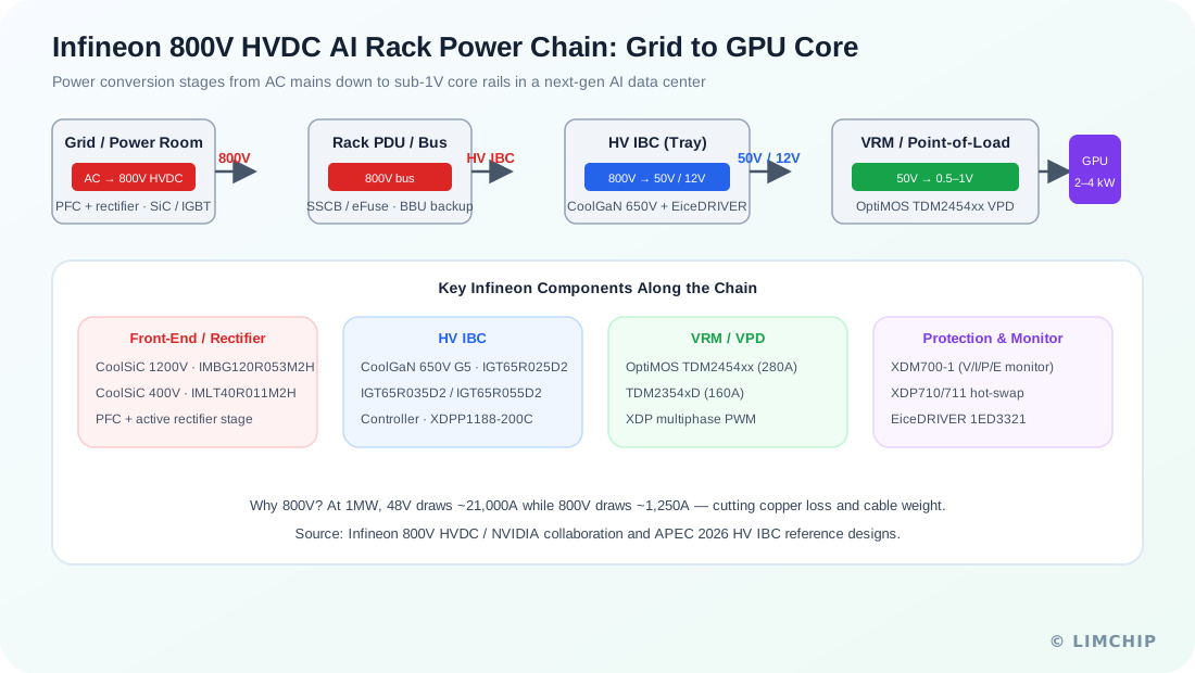
*Figure 1: Infineon's proposed grid-to-core power chain for AI data centers, using 800V HVDC distribution, HV IBCs, and vertical point-of-load delivery.*
The three main routes from 800V to the GPU #
Infineon describes three ways to convert 800V down to the low-voltage rails used by GPUs. Each route makes a different trade-off between efficiency, component count, and PDN stress.
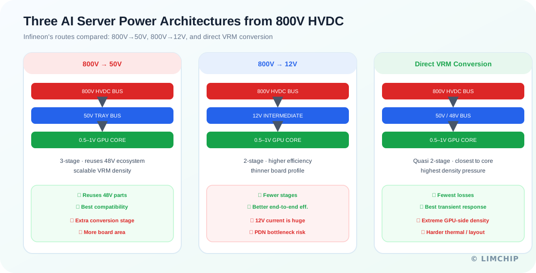
*Figure 2: Three candidate architectures from 800V HVDC to the GPU core rails. Infineon's 800V→50V route is the most ecosystem-friendly; 800V→12V is more compact but faces PDN bottlenecks; direct VRM conversion is the highest-density option.*
800V → 50V (three-stage, ecosystem-friendly) #
This is the route Infineon appears to favor for near-term adoption (our read of Infineon's published reference designs, not an official commitment). The rack carries 800V DC. A high-voltage intermediate bus converter (HV IBC) drops it to 50V for the tray. A low-voltage IBC or VRM then supplies the GPU at its final 0.5V–1V rails.
Pros:
- Reuses much of the existing 48V/50V ecosystem, including connectors, VRM controllers, and board designs.
- Distributes power conversion across more stages, which keeps each stage within a manageable temperature and density envelope.
- Lets engineers optimize the VRM for the GPU without redesigning the rack-level bus.
Cons:
- More conversion stages mean more devices and slightly more cumulative loss.
- Needs both a high-voltage IBC and a low-voltage IBC/VRM.
Infineon's 800V→50V reference design uses two 3 kW 400V-to-50V converter blocks in an input-series-output-parallel (ISOP) arrangement, built around 650V CoolGaN switches, EiceDRIVER gate drivers, and a PSOC microcontroller. In that reference design, the demo unit measures 60 × 60 × 11 mm and achieves >98% efficiency at full load with a power density of about 2.5 kW/in³ — figures quoted for the reference design, not a generic industry average.
800V → 12V (two-stage, compact but current-heavy) #
Here the 800V bus is converted directly to a 12V intermediate rail, and then VRMs step down to the GPU core voltages. This removes one conversion stage and can improve end-to-end efficiency.
Pros:
- Fewer stages than the 50V route.
- Enables a thinner server board profile because the intermediate bus is at low voltage near the GPUs.
Cons:
- 12V current becomes extremely high at multi-kW GPU loads, making the PDN a real bottleneck.
- VRMs must be rated for 12V input, and the PCB copper weight and connector sizing become critical.
- Thermal stress concentrates at the VRM stage.
Infineon's 800V→12V reference design uses a matrix transformer in an ISOP half-bridge LLC topology, measuring 130 × 40 × 8 mm. It delivers 6 kW continuous power and peaks to 10.8 kW for 400 µs, with 98.2% peak efficiency and 97.1% full-load efficiency. Power density exceeds 2.3 kW/in³.
Direct VRM conversion (quasi two-stage, most aggressive) #
In this approach, the converter steps directly from the intermediate 50V bus to the GPU core voltage without an extra 12V stage. The converter sits very close to the GPU, often as part of a vertical power delivery (VPD) module under the processor package.
Pros:
- Fewest conversion losses.
- Fastest transient response because the output inductor is close to the load.
- Best power density in terms of power delivered per square millimeter of board area.
Cons:
- Demands extreme component density and thermal management near the GPU.
- Magnetic design becomes more complex.
- Less forgiving for layout and EMI.
This is where Infineon's VPD modules and advanced magnetics come in.
PDN is the real bottleneck, not conversion efficiency #
The PDN includes all the copper, vias, connectors, capacitors, and inductors between the power supply output and the GPU silicon. At 2–4 kW per GPU with millisecond-scale load transients, the PDN must handle thousands of amps while keeping voltage droop within a tight tolerance.
Traditional horizontal power delivery routes current across the motherboard surface. VPD (vertical power delivery) moves the power stage directly underneath the processor, cutting the resistive path. Infineon estimates that VPD can reduce the distance power travels through the PCB, lowering resistive losses and improving both thermals and transient response.
For buyers, the practical implication is that power modules, VRM controllers, and bulk capacitors are no longer interchangeable commodities. The exact package, footprint, and current rating determine whether a module can be tiled around a next-generation GPU.
GaN and SiC: why wide bandgap matters here #
Higher voltage and higher switching frequency both point toward wide-bandgap devices. Infineon's portfolio uses three materials across the chain:
- SiC (CoolSiC): used for the 800V AC-DC rectification and high-voltage primary side because of its high voltage rating and low switching losses. The 1200V CoolSiC G2 MOSFETs are typical candidates for the front end.
- GaN (CoolGaN): used in the HV IBC because it enables very high-frequency switching with lower gate charge and lower RDS(on) loss than silicon at the same voltage. In Infineon's HSC prototype, replacing Si FETs with GaN FETs cut the number of top-side switches from 8 to 4 while keeping efficiency nearly identical at 1 kW (difference ~0.15%).
- Silicon (OptiMOS): still used for the final VRM stage, where 40V-class synchronous FETs need very low RDS(on) and mature, low-cost packaging.
HSC: the topology Infineon is pushing for density #
HSC stands for Hybrid Switched Capacitor. It combines elements of a switched-capacitor converter with a transformer-based converter to balance power density, efficiency, and magnetic loss.
In the Infineon HSC prototype, a 1.3 kW module uses a transformer ratio of 8:1 in a 42 × 18 × 7.7 mm package. GaN devices are introduced to reduce the output impedance during the dead time, which is one of the main loss mechanisms in HSC stages. The result is a topology that can compete with LLC resonant converters for intermediate bus conversion while enabling a thinner, more modular form factor.
VPD modules: the part buyers will actually order #
Infineon's OptiMOS power module family is the clearest bridge from architecture to bill of materials. The current third-generation part is the TDM2454xx series:
- Quad-phase module, up to 280 A peak in a 10 × 9 × 5 mm package.
- Claims >2.0 A/mm² thermally derated current density.
- Designed for true vertical power delivery, with a footprint that can be tiled in arrays around the GPU.
- Integrates embedded capacitors in the package to reduce external capacitor count.
Earlier generations include the TDM2354xD/T dual-phase 160 A modules and the TDM2254xD dual-phase 140 A modules. Buyers replacing older modules with TDM2454xx should verify the land pattern, pinout, and current-sense interface, because the newer packages are optimized for tiling and may not be drop-in compatible.
Key orderable part numbers for buyers #
The following table maps Infineon parts to the stages of an 800V HVDC AI server. Suffixes and exact package codes vary by reel type and grade; always confirm the full orderable OPN before BOM freeze.
| Stage | Part number | Description | Key specs | Package |
|---|---|---|---|---|
| HV rectifier | IMBG120R053M2H | CoolSiC 1200V G2 MOSFET | 53 mΩ, 175°C | D²PAK-7 |
| HV rectifier | IMLT40R011M2H | CoolSiC 400V G2 MOSFET | 11 mΩ | TOLT |
| HV IBC switch | IGT65R025D2 | CoolGaN 650V G5 HEMT | 25 mΩ | TOLL |
| HV IBC switch | IGT65R035D2 / IGT65R055D2 | CoolGaN 650V G5 HEMT | 35 / 55 mΩ | TOLL |
| HV IBC controller | XDPP1188-200C | Digital power controller | 48V/24V/12V, up to 800V | VQFN |
| Gate driver | 1ED3321MC12N | Isolated SiC/GaN driver | 2.3 kV isolation | DSO-16 |
| Gate driver | 1ED3142MU12F | 6.5 A isolated driver | 3 kV rms | DSO-8 |
| VRM / VPD | TDM2454xx | Quad-phase VPD module | 280 A, 2.0 A/mm² | 10 × 9 × 5 mm |
| VRM / VPD | TDM23541D | Dual-phase VPD module | 160 A | 8 × 8 × 4 mm |
| Monitor | XDM700-1 | 12-bit V/I/P/E monitor | 80V input, PMBus 1.3 | VQFN-24 |
| Protection | XDP710-002 | Hot-swap controller | 80V, digital SOA | VQFN-29 |
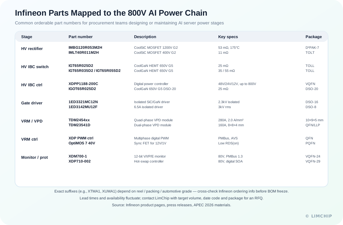
*Figure 3: Infineon orderable part numbers mapped to the 800V HVDC AI server power chain. Suffixes and exact packaging codes should be verified before ordering.*
Performance snapshot: density and efficiency #
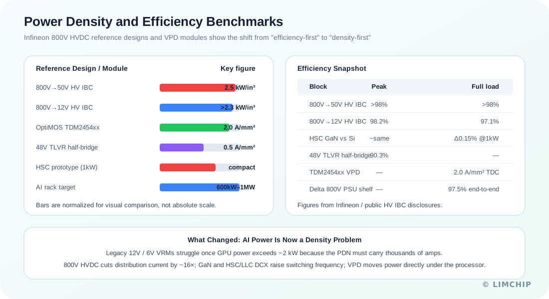
*Figure 4: Power density and efficiency benchmarks from Infineon's 800V HVDC reference designs and VPD modules. The data shows the shift from efficiency-first design to density-first design in AI power systems.*
Key numbers to remember (all from Infineon's reference designs and product briefs, not generic industry averages):
- 800V→50V HV IBC: 60 × 60 × 11 mm, 2.5 kW/in³, >98% efficiency at full load.
- 800V→12V HV IBC: 130 × 40 × 8 mm, >2.3 kW/in³, 98.2% peak / 97.1% full-load efficiency.
- TDM2454xx VPD: 280 A quad-phase in 10 × 9 × 5 mm, >2.0 A/mm² current density.
- 48V TLVR half-bridge: 90.3% peak efficiency, 0.5 A/mm² density.
Supply chain and sourcing notes for buyers #
Availability and lead time #
800V HVDC AI power components are still in the early deployment phase. Reference designs are announced, but mass production depends on hyperscaler adoption and the timing of NVIDIA's next-generation rack platforms. As of mid-2026, lead times for comparable CoolGaN, CoolSiC, and XDP controllers are typically cited in the range of 16–40 weeks, with longer tails for automotive-grade or specific package variants. Always lock the date-code window with the distributor or contract manufacturer before placing a long-lead RFQ.
Package and footprint verification #
- TDM2454xx and TDM2354x modules are not drop-in compatible with each other. Pinout, thermal pad size, and current-sense configuration differ.
- CoolGaN G5 devices are available in TOLL, TOLT, and DSO-20 packages. The RDS(on) rating is not the only variable; gate-drive requirements and layout parasitics change with the package.
- CoolSiC G2 MOSFETs come in TOLL, TOLT, D²PAK-7, and TO-247-4 packages. The 1200V devices are needed for the 800V primary side; the 400V devices are used in lower-voltage bridges.
Grade and suffix #
Suffixes like XTMA1, XUMA1, or HXKSA1 indicate packing, reel configuration, and temperature/grade variants. Automotive-grade parts (prefixes starting with A) are not necessary for data-center equipment but sometimes appear in the same supply pool. Verify the full OPN before buying.
Cross-reference caution #
Infineon is not the only supplier in this space. On the SiC side, Wolfspeed, STMicroelectronics, onsemi, and ROHM offer competing 1200V MOSFETs. On the GaN side, Navitas, EPC, Innoscience, and Texas Instruments are also active. If a design is qualified for a specific Infineon gate driver or GaN FET, switching vendors usually requires a re-qualification because gate-drive timing and layout parasitics differ significantly.
Sourcing strategy #
For a new AI power design, the highest-risk parts are usually the TDM2454xx VPD modules, XDPP1188-200C controllers, and CoolGaN 650V G5 FETs in low-RDS(on) packages. These should be ordered first and in larger buffer quantities if the build schedule is aggressive. SiC front-end devices and gate drivers tend to have more second-source options, though matching performance requires engineering review.
FAQ #
Q: Is 800V HVDC already shipping in production AI data centers? A: First-generation deployments are reported for 2026–2027, led by hyperscalers and NVIDIA partners. Broader, mass-market adoption is an industry expectation later in the decade as GPU racks cross the 600 kW mark, not a confirmed production timeline.
Q: Does 800V HVDC replace the 48V rack entirely? A: Not immediately. 800V is the rack-level backbone. Inside the tray, 48V/50V or 12V intermediate buses are still used, depending on the architecture route.
Q: Why use GaN instead of SiC in the IBC? A: GaN is better suited for the high-frequency, medium-voltage switching of the IBC because of its low gate charge and fast switching. SiC is usually preferred for the higher-voltage, lower-frequency AC-DC rectification stage.
Q: Are the TDM2454xx modules compatible with older TDM2254x or TDM2354x modules? A: No. Verify the footprint, pinout, and control interface before swapping.
Q: What should I verify before issuing an RFQ for these parts? A: Exact OPN including suffix, target date-code window, package type, required quantity, and whether the parts are for engineering samples or production. For VPD modules, also confirm the intended GPU platform and current rating.
LimChip sourcing advice #
Infineon's 800V HVDC roadmap is a useful signal for buyers even if your current builds are still 48V-based. The shift toward higher density and higher current per module will tighten supply for the parts listed above, especially CoolGaN and VPD modules. If you are planning a 2026–2027 AI server or power-module build, consider securing samples and first-production lots early, and qualify second-source packages wherever the electrical margins allow.
For production-scale orders, RFQ with the exact OPN, target quantity, date-code window, and destination. We can also support cross-reference checks for SiC and GaN devices if a primary part is unavailable.
Designs that retain a 48V or 54V tray bus also need a separately verified input protection stage; see the 54V AI server hot-swap and backplane protection guide for inrush, MOSFET SOA, fault turn-off and exact controller order codes.
For the conversion stage itself, the 800VDC-to-54V/12V isolated DC/DC design guide separates the published 50V and 12V reference-design evidence from a production 54V output contract, and covers ISOP balance, isolation and fault ownership.
RFQs welcome. RFQ: sales@limchip.com
Sources #
- Infineon. Infineon to revolutionize power delivery architecture for future AI server racks with NVIDIA, May 2025.
- Infineon. CoolGaN-based HV IBC reference designs for 800 VDC architectures in AI data centers, March 2026 — source for the 800V→50V and 800V→12V reference-design figures (>98% / 2.5 kW/in³, 98.2% peak, 60×60×11 mm, etc.).
- Infineon. Product pages for CoolGaN 650V G5, CoolSiC 400V/1200V G2, OptiMOS TDM2454xx VPD modules, XDM700-1 monitor and XDP digital power controllers — part numbers cited above are from Infineon's published portfolios.
- Infineon Community, "DC/DC Power Architecture for 800V AI Server Racks," 2026.
Need stock, date-code or package confirmation?
Send the part number, quantity, target date code and packaging requirements. LimChip will check available lots and RFQ details before you place the order.
Send RFQ