
Article contents0%
- Why a course assignment belongs on a sourcing blog
- What actually runs on the board
- Establish the golden answer before touching hardware
- INT8: the "sticky note" compression
- Eleven dedicated workshops, not one factory
- The FAIL screenshot is the product
- Energy per token: a different leaderboard
- AI wrote the cores; humans kept the gate
- The real thesis: custom domain-specific LLM chips
- Multi-FPGA LLMs: the academic track is already paved
- What buyers should note
- Six things to take away
- Sources
Why a course assignment belongs on a sourcing blog #
A university instructor turned "fit a Transformer into an FPGA" into an undergraduate capstone. Four students shipped a working 6-layer nanoGPT on an AMD Xilinx Zynq UltraScale+ MPSoC (xczu7ev) — 3.9 W on-chip, no OS, no network, no GPU. The reason we cover it here is not the novelty of running a language model on an FPGA (that has been done). It is the *engineering discipline* the project demonstrates, and what that discipline tells component buyers about the real constraints of on-device AI silicon.
This article is our procurement-oriented read of the published project. All experimental figures — 777 ms per token, 3.9 W, LUT/DSP utilization, the 95.5% matmul share — are quoted per the project report and its open-source repository, not presented as generic industry numbers. These figures are results from the reported project configuration, not general specifications of the XCZU7EV platform. Source is credited at the end.
What actually runs on the board #
The blue line of the demo is a Shakespeare-flavored chat over a serial terminal. The board answers in iambic cadence. It is charming, and it is also the trap: a 3.9 W model should not speak that cleanly. The firmware's own stats expose why — `PL_matmul_calls = 1` per reply. A full 6-layer model needs ~73 matmul calls per token on this implementation. So the fluent demo is a *hardware-in-the-loop showcase*, while the genuine full-model run is printed separately and, honestly, marked FAIL.
That separation — demo vs. truth, both on screen — is the most valuable thing in the whole project.
Establish the golden answer before touching hardware #
The students started from Karpathy's nanoGPT: 6 layers, 384 dims, a 65-character vocabulary, trained on Shakespeare. The real deliverable was not the model. It was a layer-by-layer golden reference — every layer's input and output archived — so that each later hardware step could be checked against a known-correct answer.
For buyers, the parallel is direct: a trusted reference (datasheet curves, an ATE report, a known-good batch) is what turns "the part works" from a feeling into a checkable claim.
INT8: the "sticky note" compression #
32-bit floats are too fat for the fabric. The team used INT8 quantization, collapsing weights to 8-bit fixed point — roughly 4× thinner, with perplexity regression kept under ~10% per the report. Weights, scales, and golden values were exported as a shared C header so software and hardware "keep one ledger."
Quantization is now the default move for edge inference parts (NPUs, DSP-rich FPGAs, microcontrollers). When you source for an edge-AI BOM, ask for the quantization recipe, not just the raw TOPS.
Eleven dedicated workshops, not one factory #
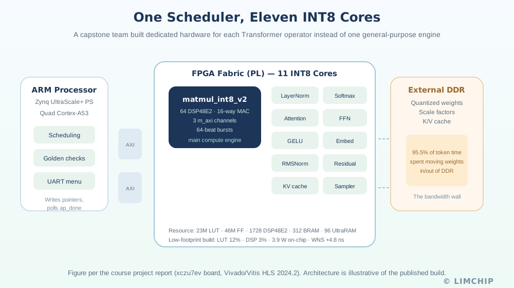
A GPU is a general-purpose factory. This team built eleven INT8 accelerator cores, one per Transformer operator, in Vitis HLS:
- `matmul_int8_v2` — the main engine: 64 DSP48E2, 16-way MAC, three independent `m_axi` channels, 64-beat bursts to saturate DDR bandwidth.
- Plus LayerNorm, Softmax, Attention, FFN, GELU, Embed, RMSNorm, Residual, KV-cache, and Sampler cores.
All eleven close timing at 100 MHz; C-synthesis estimated a 7.3 ns critical path (~137 MHz ceiling, ~37% margin). The verification went further: post-synthesis netlist re-simulated in QuestaSim with INT8 boundary values (−128, 127), 100% statement coverage.
Two builds were reported on the same xczu7ev:
- Low-footprint (delivered): LUT 12%, FF 8%, BRAM 4%, DSP only 3%; WNS +4.786 ns; 3.901 W on-chip.
- High-footprint (explored): four `matmul_int8_v2` in parallel; LUT 52%, DSP 46%; WNS +1.614 ns; 4.612 W.
Same device, same verification flow, both timing-clean. Shipping one stable build and exploring one faster build is risk management that reads as senior, not student.
The FAIL screenshot is the product #
The full-model run prints exactly what you would hope a senior engineer would surface:
``` avg_ms_per_token = 777 (target ≤ 200) status = FAIL / PARTIAL ```
And the time breakdown: 95.5% of the 777 ms is matrix multiply — specifically, weights shuttling in and out of DDR. Not slow multipliers. Too many trips to the warehouse. The firmware auto-flags the run as FAIL rather than hiding it.
This is the bandwidth wall, stated by measurement instead of slogan.
Energy per token: a different leaderboard #
On raw latency, an RTX 5090 at ~1.93 ms/token crushes the field. But rank by energy per token and the winner changes. At the project's 200 ms *acceptance target* — an estimate, not a board-level measurement — the small FPGA build is estimated to draw ≤ 780 mJ per token, beating far larger platforms on efficiency. This figure is a first-order estimate from 3.9 W on-chip × 200 ms; it is not a measured per-token benchmark, and the 777 ms unoptimized run would not hold this lead.
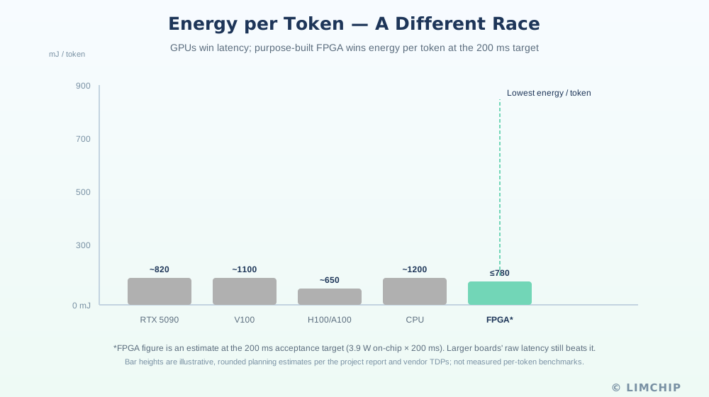
The takeaway for sourcing: "fast" and "efficient" are different purchase orders. Phones, robots, satellites, and hearing aids have neither a 575 W budget nor space for a GPU fan. That is the next landing zone for on-device models.
AI wrote the cores; humans kept the gate #
How did undergraduates finish this in a semester? The report's "AI co-development" section: all eleven cores were first drafted from natural-language specs by an AI coding assistant, then iterated against synthesis feedback until they passed. AI produces; humans gate. The gate is not a slogan — it is concrete: a layer-by-layer golden reference, boundary-value simulation (INT8 −128/127, 100% statement coverage), and an acceptance test that auto-flags a run as FAIL rather than hiding it. A real delivery carries the verification chain — golden reference, simulation, checksums and acceptance testing — so the evidence is checkable, not trusted.
They even added an unassigned extra: deploying LeNet-5 digit recognition via hls4ml, 10/10 test images correct.
The real thesis: custom domain-specific LLM chips #
Public reports describe a February 2026 development from Taalas: baking Llama 3.1 8B directly into silicon (TSMC 6 nm, 815 mm², 53 billion transistors, ~14,000–17,000 token/s per user, ~200 W), with a reported ~2-month turnaround for a new model using two metal-mask revisions. LimChip has not independently verified these figures; they are presented as reported industry information, not product specifications.
That is the same lesson as the FAIL screenshot: inference is ~95% moving weights, not computing. Stop moving them and speed jumps by 1–2 orders of magnitude.
The proposed path — custom domain-specific LLM chips — distills a field's expertise into a ~3B model, quantizes to INT4 (~1.5 GB), and fixes it into HBM-backed FPGA or ASIC. Token is unlimited, fast, and data-never-leaves. Best-fit domains share four traits: narrow vocabulary, closed task, latency/privacy sensitivity, no open-world knowledge (network security, industrial maintenance, space/unmanned, medical/legal, offline education).
Multi-FPGA LLMs: the academic track is already paved #
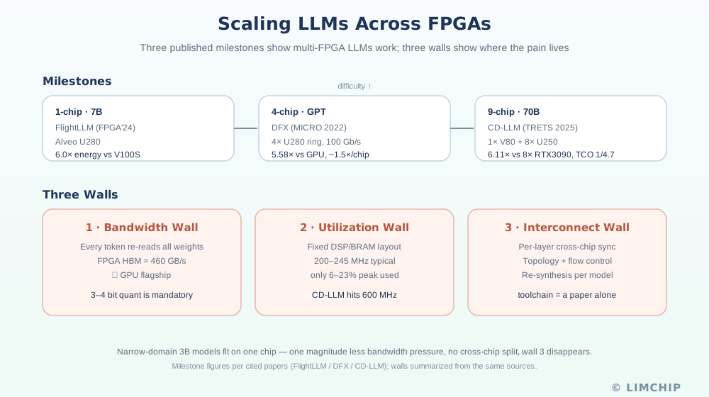
Skeptical that a few FPGAs can run a real LLM? The literature says otherwise:
- 1-chip 7B — FlightLLM (FPGA'24): Alveo U280, weight-stays-on-chip decode; 6.0× energy vs V100S, 1.8× cost-effectiveness, Versal variant beats A100 on throughput.
- 4-chip GPT — DFX (MICRO 2022): four U280 in a 100 Gb/s ring; 5.58× vs GPU, 3.99× energy; ~1.5× per added chip (communication taxes the ideal 2×).
- 9-chip 70B — CD-LLM (TRETS 2025): one V80 (HBM, attention) + eight U250 (matmul); Llama-3.1-70B at avg 3.45-bit; 6.11× vs 8× RTX3090, TCO down 4.71×.
Three walls remain, and they are the sourcing constraints buyers should internalize:
1. Bandwidth wall — every token re-reads all weights; FPGA HBM ≈ 460 GB/s, a fraction of flagship GPU. 3–4 bit quantization is mandatory, not optional. 2. Utilization wall — fixed DSP/BRAM placement caps most designs at 200–245 MHz, only 6–23% of peak; CD-LLM's compute-specialized layout reaches 600 MHz. 3. Interconnect wall — per-layer cross-chip sync, custom topology/flow control, and hours of re-synthesis per model.
Narrow 3B models fit on one chip: one magnitude less bandwidth pressure, no cross-chip split, wall 3 vanishes. That is precisely why domain-specific small models are the gentler slope.
What buyers should note #
- xczu7ev / Zynq UltraScale+ MPSoC remains a capable, widely available embedded-AI platform, but lead times and allocation on 16 nm UltraScale+ can stretch — plan early for production.
- HBM-backed FPGAs (Versal V80, Alveo U280/U250 class) are the parts that actually relieve the bandwidth wall. They are scarce and pricey; qualify second sources early.
- Quantization recipe + verification assets (golden vectors, boundary cases) are part of the deliverable, not paperwork. Request them.
- "Custom domain LLM chip" is no longer science fiction — Taalas and the multi-FPGA papers show a credible, if narrow, path. If your application fits the four traits above, it is worth a design exploration, not a wait-and-see.
LimChip does not stock the xczu7ev education board, but we source Zynq UltraScale+ and Versal families for production. If you are building embedded-AI hardware, open an RFQ and we will map availability and lead times.
Six things to take away #
1. Set the ruler first; then build — archive a golden reference before writing hardware. 2. Put acceptance in the deliverable — one key reproduces every claim. 3. Demo and truth, both on screen — honest FAIL beats fluent fiction. 4. Speed and efficiency are two races — GPUs win latency; dedicated hardware wins energy per token. 5. AI co-development: AI produces, humans gate — denser verification, larger leverage. 6. Custom domain-specific LLM chips are open — narrow model + fixed weights + a few FPGAs beats a datacenter for the right problem.
Sources #
- Source: 网络交换FPGA 微信公众号,原文系列《把大模型塞进FPGA》。
- Open-source project repository: zcxsince2005 / My_Transformer_on_fpga.
- Device reference: AMD Xilinx Zynq UltraScale+ MPSoC product documentation.
- Taalas HC1 information: EE Times and heise reports.
All board-level numbers (777 ms/token, 3.9 W, utilization, 95.5% matmul) are results from the reported project configuration, not general specifications of the XCZU7EV platform. Energy-per-token figures are estimates at the 200 ms acceptance target and are not board-level measurements.
Need stock, date-code or package confirmation?
Send the part number, quantity, target date code and packaging requirements. LimChip will check available lots and RFQ details before you place the order.
Send RFQ