

Why IC package type matters #
An integrated circuit is more than its electrical function. The package decides how the device sits on the PCB, how it is soldered, how heat leaves the chip, how easily it can be inspected and how risky it is to source from open-market inventory.
For buyers, package type is also a part-number control issue. A similar-looking part number may have a different body, pin count, packing method, moisture sensitivity level or approved footprint. Before purchase, confirm the full manufacturer part number, package code and packing condition rather than relying on a short description.
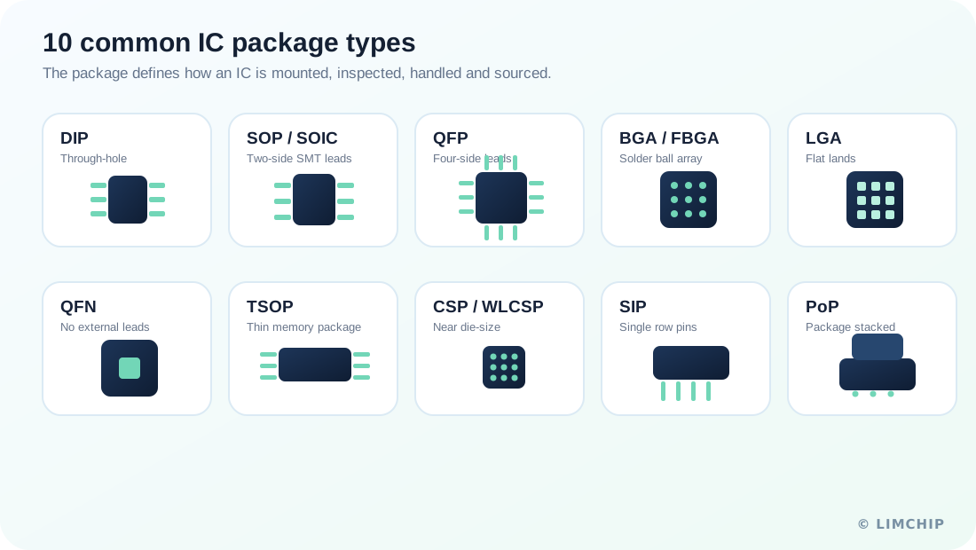
1. DIP — Dual In-line Package #
DIP is a through-hole package with two parallel rows of pins. It is large, simple and easy to handle, which is why it is still common in education, development boards, legacy industrial equipment and some socketed designs.
Its sourcing risk is usually not complexity. The real checks are date code, lead oxidation, bent pins, storage condition and whether older stock is acceptable for the project.
2. SOP / SOIC — Small Outline Package #
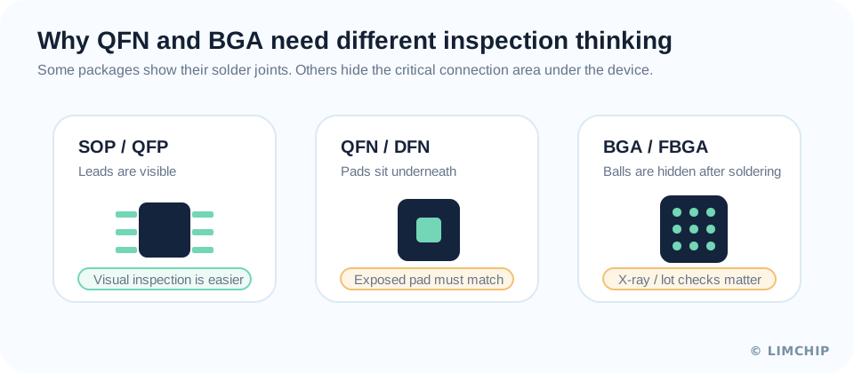
SOP and SOIC are surface-mount packages with leads on two sides. They are common for analog ICs, logic, drivers, memory, small regulators and interface devices. The solder joints are visible, so inspection is easier than with QFN or BGA.
Do not treat every two-sided package as the same. Body width, pin pitch, pin count and suffix can change the footprint. For RFQ work, confirm whether the approved part is reel, cut tape, tube or tray.
3. QFP, LQFP and TQFP — Quad Flat Packages #
QFP packages have leads on all four sides. LQFP and TQFP are common variants used for microcontrollers, DSPs, controllers, audio ICs, communication devices and embedded platforms.
The advantage is visibility: the leads can be inspected and rework is possible. The weakness is mechanical handling. Fine-pitch leads bend easily, so tray condition, packing method and package photos matter for shortage or open-market stock.
4. BGA and FBGA — Ball Grid Array #
BGA packages use solder balls under the device instead of visible side leads. This supports high pin count, compact routing and better electrical performance for high-speed devices. FBGA is common in memory and other compact IC packages.
BGA is important in CPUs, GPUs, DRAM, NAND, eMMC, UFS, FPGAs, SoCs and networking ASICs. It is also one of the package families where sourcing risk is higher. Reballing, remarking, mixed lots and removed-board material can be hard to identify by top marking alone.
For high-value BGA/FBGA parts, request label photos, package photos, lot and date-code confirmation. For critical projects, X-ray or deeper inspection may be appropriate.
5. LGA — Land Grid Array #
LGA packages use flat contact lands instead of pins or solder balls. Many socketed desktop and server processors use LGA-style contact systems, and smaller LGA packages also appear in RF modules, MEMS sensors and compact modules.
The buyer check is contact condition and exact platform fit. LGA parts can look similar, but socket, generation, mechanical keying, power requirements and thermal solution may make them incompatible.
6. QFN and DFN — No-lead Packages #
QFN has contact pads around the underside edge of the package and often a large exposed thermal pad. DFN is similar but usually has contacts on two sides. These packages are compact, thermally efficient and common in PMICs, RF ICs, sensors, current-sense amplifiers and small converters.
The challenge is inspection. Pads are not as visible as gull-wing leads, and the thermal pad depends on correct solder paste and reflow. Confirm the exact package code, exposed-pad layout, MSL status and packing condition before accepting a substitute.
7. TSOP — Thin Small Outline Package #
TSOP is a thin, two-sided surface-mount package. It was widely used in memory devices such as Flash and SRAM before many designs moved toward BGA-style packages.
For sourcing, TSOP often appears in older or legacy BOMs. Buyers should check whether the part is active, discontinued, old date code or recovered inventory. Package width and pin count should be confirmed against the approved BOM.
8. CSP and WLCSP — Chip Scale Packages #
CSP packages are close to the size of the silicon die. WLCSP goes further by forming the package at wafer level. These packages are very small and useful in mobile, wearable, RF and compact sensor products.
Small size creates handling risk. Fine pitch, moisture control, board flex, underfill requirements and rework capability should be considered before accepting alternate stock.
9. SIP — Single In-line Package #
SIP packages use one row of pins. They are narrow and simple, often seen in older modules, resistor networks, optocouplers, hybrid ICs, relay modules and vertical board-space layouts.
The practical sourcing checks are pin condition, lead spacing, package height and whether the current project accepts the same mechanical form as the original design.
10. PoP — Package on Package #
PoP stacks one package on top of another, often with a processor or SoC below and memory above. It saves PCB area and is common in compact mobile and embedded systems.
PoP is not a casual substitute item. Stack compatibility, thermal design, assembly process and exact approved part number matter. If the BOM calls for a specific PoP combination, confirm the full orderable code and do not quote a nearby part without engineering approval.
Quick package reference #
| Package | What it looks like | Buyer check |
|---|---|---|
| DIP | Two rows of through-hole pins | Date code, lead condition, socket fit |
| SOP / SOIC | Two-side gull-wing SMT leads | Body width, pin count, reel/tube code |
| QFP / LQFP / TQFP | Leads on four sides | Fine-pitch lead condition and tray packing |
| BGA / FBGA | Solder balls under the package | Source, reballing risk, X-ray or lot checks |
| LGA | Flat contact lands | Socket/platform fit and contact condition |
| QFN / DFN | No long external leads | Exposed pad, MSL, reflow and package code |
| TSOP | Thin two-side memory package | Legacy status, package width, pin count |
| CSP / WLCSP | Near die-size package | Handling, moisture, fine-pitch assembly |
| SIP | One row of pins | Height, lead spacing, mechanical fit |
| PoP | Stacked packages | Approved stack, thermal and assembly control |
Package checks before RFQ #
- Confirm the full manufacturer part number and suffix.
- Match package / case, pin count, pitch and body size to the approved BOM.
- Confirm packing format: reel, tray, tube, cut tape, dry pack or bulk.
- Check date code, lot consistency and acceptable country of origin.
- Ask for package photos when stock is high value, shortage-driven or not from
an authorized channel.
- Treat QFN, DFN, BGA, FBGA, CSP and WLCSP as inspection-sensitive packages.
- Do not accept a package change unless engineering approves it.
Related reading #
For a deeper procurement-focused view, see the LimChip guide: IC Package Types Explained: A Buyer’s Guide to DIP, SOIC, QFP, QFN, BGA and CSP.
Procurement takeaway #
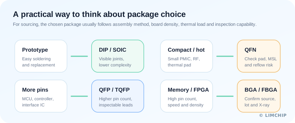
Package type is not just a visual detail. It affects footprint, soldering, inspection, rework, thermal behavior, moisture handling and sourcing risk.
For ordinary parts, package checks prevent wrong-footprint orders. For memory, FPGA, processor, RF and power devices, package checks also help control counterfeit, reballing, remarking and lot-mixing risk.
Need stock, date-code or package confirmation?
Send the part number, quantity, target date code and packaging requirements. LimChip will check available lots and RFQ details before you place the order.
Send RFQ